The Price of Memory in China
A memory maker is now the most valuable listed company in China. For what that has to do with the price of an older GPU, read the tea leaves on both sides of the strait.
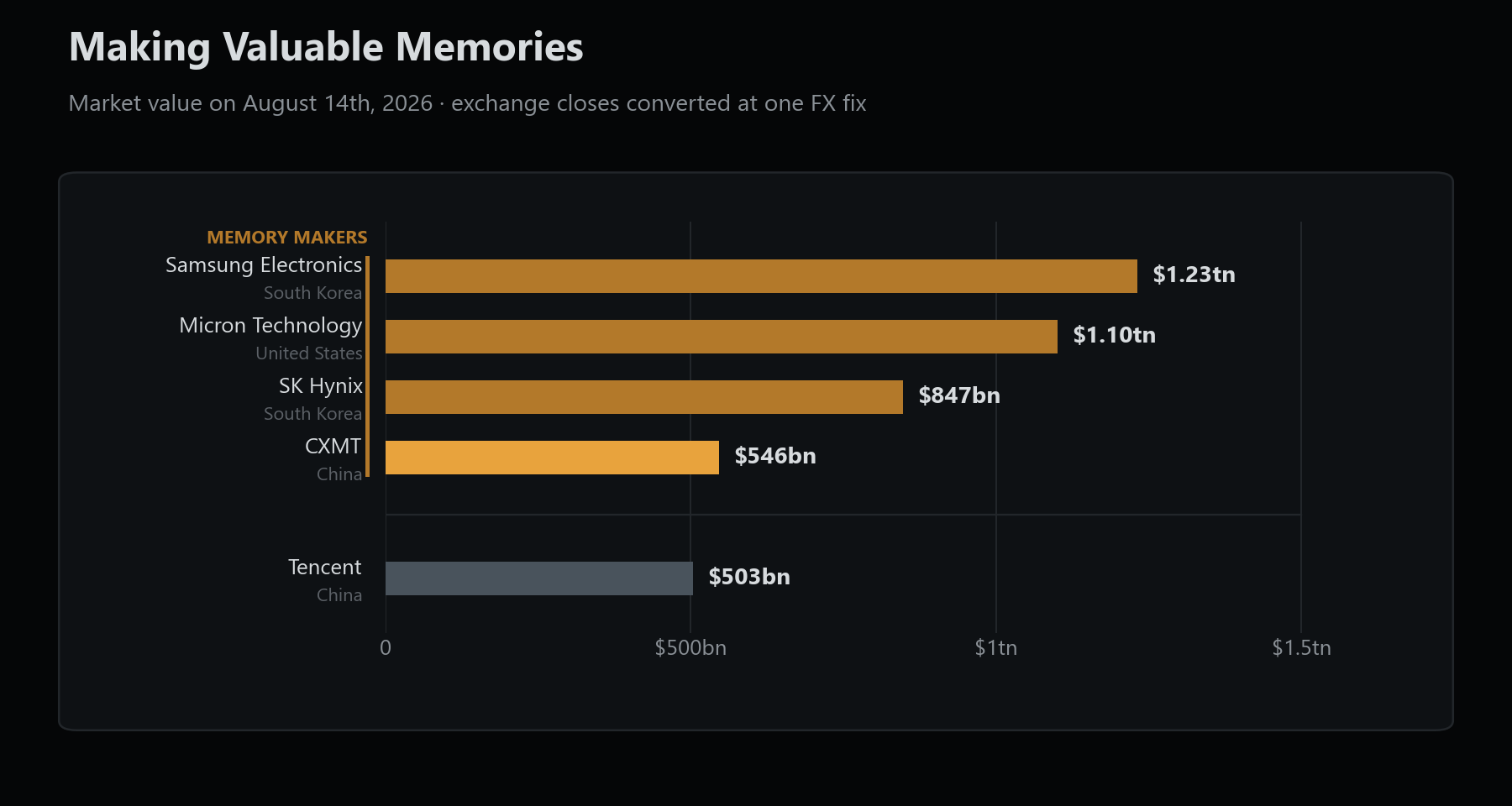
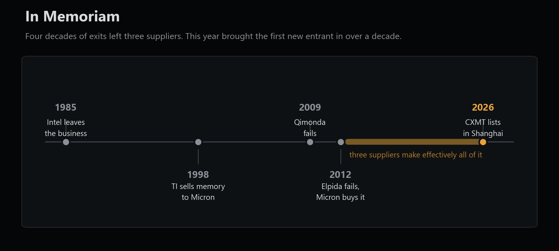
ChangXin Memory Technologies (CXMT) closed the end of last week valued at near $546 billion, 18 days after its Shanghai listed IPO near $86 billion. Less than one month ago another memory maker headquartered in South Korea, SK Hynix, listed on Nasdaq and its prospectus shows first-quarter 2026 DRAM bit volume flat against roughly a 65% price increase. That industry consolidated to three suppliers and has not added a new one in over a decade.
Basis
Exchange closes on August 14th, 2026 converted at one FX fix. Each figure divided by that day’s share price returns the issuer’s share count, so every bar is recomputable. Tencent makes no memory; it is here because it is the company CXMT passed.We all continue to see the demand for global compute expanding at breakneck pace. The market paid roughly 65% more for the same volume of memory, then bid a company promising more of it past every other listed company in China.
Basis
Exits are dated to the announcement of withdrawal from commodity DRAM, whether by closure, sale or merger. CXMT is marked at its 2026 listing rather than at first production.As we think about this incoming supply of memory to the markets we are focused on which levers will have the most effect on the earning power of prior generation GPUs, and on what schedule.
01 Total Recall
Two Victorian lessons
In 1865 Jevons observed that more efficient steam engines raised coal consumption rather than lowering it. Each engine burned less coal, which made steam power cheap enough for uses that had never justified it. The extra demand outweighed the saving.
Eight years later the bond market that built the railroads also funded a great deal of overinvestment, and when the bubble broke the operators who came through were the ones who ran most efficiently. Microsoft's CEO cited that period on his last earnings call, telling investors 1873 is the book to read and that the job is to run an efficient railroad.
The parallel to compute in 2026 is plain to see. Each generation does more work per chip and per watt, across training and inference alike. Demand has grown through every one of those gains. GPUs six years of age are still being sold on three-year term contracts.
Demand is in line with Jevons for now. That could change from either side, and when enough new supply arrives the competition turns to price. Anyone still earning on prior generation chips then wants to be the low cost operator. That makes the incoming supply worth watching, and makes it worth knowing which attributes of a new chip would move prices most.
02 Working Memory
The attributes with the most potential to move earning power
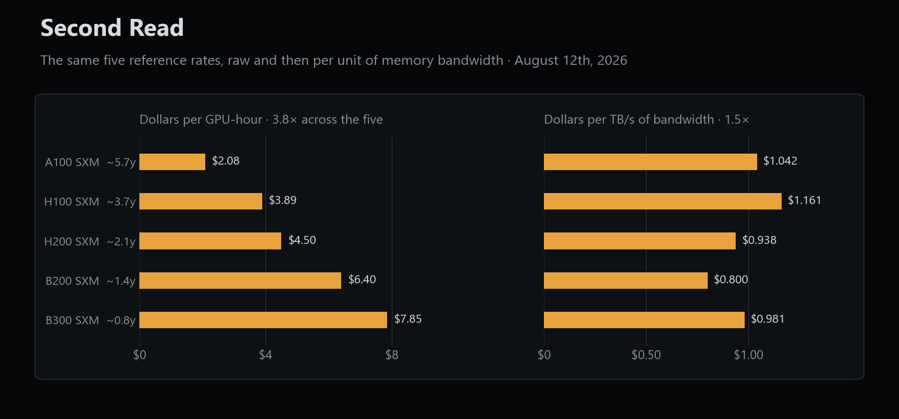
Memory capacity decides whether a model fits. Bandwidth decides how fast it runs. Power decides what it costs to keep running. Take one daily reference rate for five generations of GPUs and divide each by a figure from its spec sheet. Raw, the prices of neocloud offerings across those five generations span 3.8×, dearest over cheapest. Re-denominated, every lens compresses that:
- Per petaFLOP, 2.4×
- Per gigabyte of memory, 1.9×
- Per unit of bandwidth, 1.5×
- Per kilowatt, 1.2×
Power and bandwidth compress the cross-section hardest. Priced per kilowatt the five sit within 1.2× of one another. Memory capacity and compute compress it as well, but currently far less. The two constrained inputs of the build-out are the two that current pricing tracks most closely.
Basis
Neocloud guaranteed on-demand, all regions, 2026-08-12. Denominator is vendor nameplate memory bandwidth: 2.0, 3.35, 4.8, 8.0 and about 8.0 TB/s. Posted list asks, not transactions.Let's look at a controlled view versus current CCIR Neocloud rates: B300 holds the same 8.0 TB/s as the B200 while possessing sixty percent more memory, and is benchmarked at $7.85 against the B200's $6.40. Cheaper per gigabyte of memory, but 23 percent more expensive per unit of bandwidth. An addition to the wide attribute earned no premium on the compressed one.
Similarly the 2020 vintage A100. Scale the H100's rate by the two chips' bandwidth and the A100 prices at 90 percent of the result. Scale it by their compute and the A100 prices 71 percent above. It is the cheapest of the five per gigabyte and per kilowatt, and the dearest per petaFLOP. The market has repriced its oldest silicon tighter to its bandwidth share.
03 Memory Foam
Memory capacity supply is arriving now
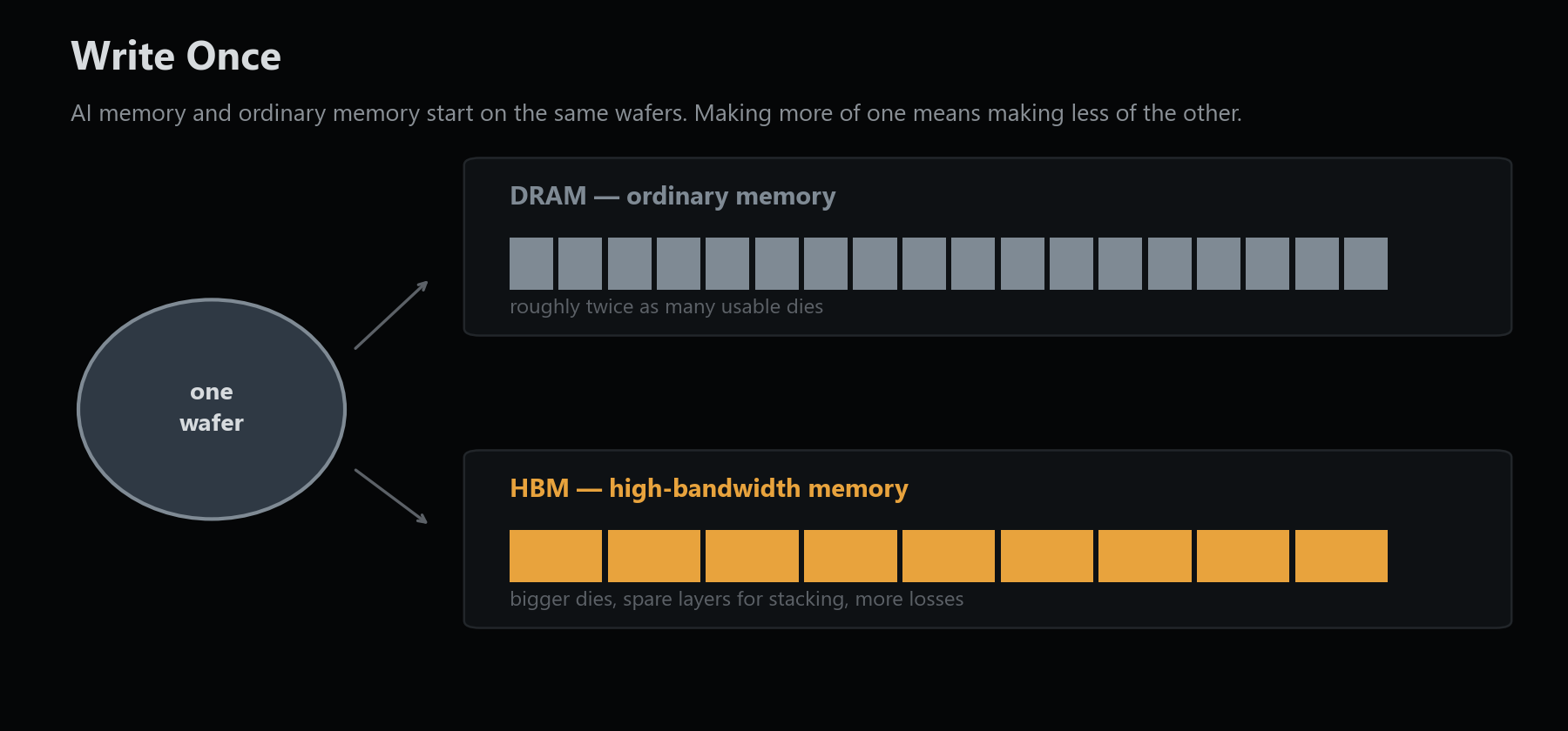
Every memory maker faces the same decision on each wafer, the silicon disc that chips are cut from and the unit a fab allocates. It can be finished as conventional DRAM, which fills the rest of an AI server, or it can be finished as high-bandwidth memory. It cannot be both, and that choice shapes the supply story.
The choice is expensive. A wafer converted to HBM yields roughly half as many usable dies, because the dies are bigger and the stacking costs spare layers and losses. A maker moving a line to HBM is giving up conventional volume to do it.
All three incumbents have been making that move. SK Hynix's own prospectus attributes the shortage in conventional DRAM to the industry-wide reallocation of production capacity to HBM.
Basis
The die ratio is a trade estimate, not a filed figure. It is directionally consistent across sources and is used here as scale, never as precision. It is quoted per DIE. Trade sources more often quote the penalty per gigabyte, where high-bandwidth memory is reported at roughly three times the wafer area of conventional DRAM.Today CXMT is adding memory volume, and capacity availability increases with it. It fills the conventional hole the incumbents leave. Its share of global DRAM bit shipments went from one percent in 2021 to nine percent in 2025, and its added volume clears largely inside China, to buyers who contracted for it in advance. Absorbing that conventional demand is what will help the conversions continue.
Reuters reports CXMT is targeting domestic HBM3 by year-end, though its prospectus names no HBM project. HBM3 is a generation behind the stacks shipping beside current accelerators, and two behind the HBM4 step now in production.
Either way, the supply arriving now lands on memory capacity, which the market prices less closely than bandwidth: 1.9× against 1.5×.
04 Photographic Memory
Bandwidth supply is scheduled
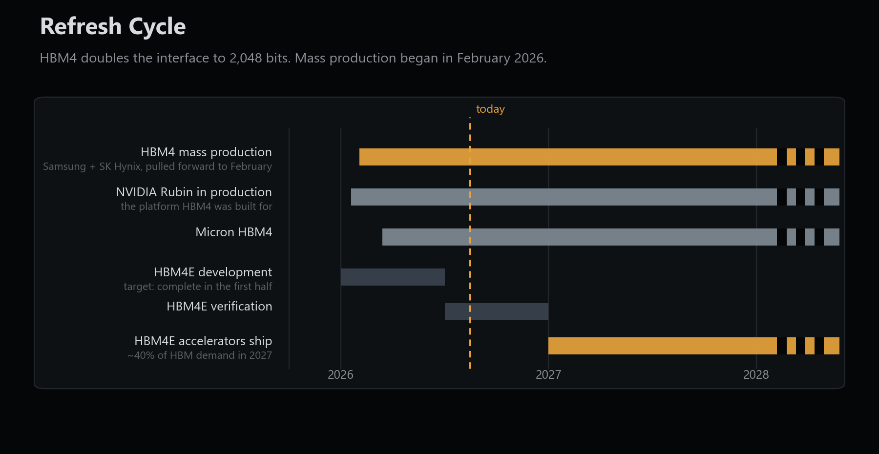
The bandwidth frontier has been flat: the B300 entered at the B200's 8.0 TB/s about seven months later. Both carry HBM3E, the stack behind every part in our panel since the H200. HBM4 is the step change, and Rubin is the part that carries it. HBM4 widens the interface from 1,024 bits to 2,048, and mass production began early this year. Rubin's published targets have run from 13 to 22 TB/s against the 8.0 that tops our panel, and the most recent revision was downward, to about 20. Treat the level as unsettled.
Through HBM3E one process built both dies in the HBM stack, the core die that stores the bits and the base die that runs the interface, and both were owned by the memory makers themselves. The wider HBM4 interface asked more of the base die than a memory process delivers, so it moved to an advanced logic node. Two companies will be using Taiwan Semiconductor Manufacturing Company (TSMC) to build that base die, and one already is.
SK Hynix sources its logic die from TSMC. Micron keeps its base die on a DRAM process through HBM4 and moves to TSMC at HBM4E. The packaging that joins finished stacks to the accelerator was already TSMC's, and it was the binding constraint on the last generation of accelerators. A foundry now sits at two points on the bandwidth path where a generation ago it sat at one.
Rentable supply is a separate question. We have not seen a public on-demand price for Rubin. Production has started and the first cloud partners are reported to take delivery this fall, with broader availability later, so we will be watching prior generation pricing as that widens.
Basis
Bands rather than dates: each of these has moved at least once.05 Refresh Rate
What is actually watchable
None of this binds while demand keeps absorbing what arrives. That is Jevons, and it has held through every efficiency gain so far. If it stops holding, the exposure is to a step change in bandwidth. HBM4 is that step change, and it increasingly runs through one foundry.
TSMC does not publish how much of that work it can do. Circulating estimates disagree by about 20%. Its own disclosed figure is a growth rate rather than a level, compounding above eighty percent from 2022 to 2027, so it tells you how fast that work is expanding and nothing about whether it is enough.
Memory capacity is arriving now, and the market prices it less closely than bandwidth. Bandwidth is where the next supply step meets a binding constraint. A generation ago the memory makers built the whole stack. It is now completed by the memory makers and TSMC together. Our read is that prior generation chips are more exposed to that step than to one in memory capacity or compute.
Notes on sources and construction
Rental rates. Neocloud guaranteed on-demand, all regions, SXM parts throughout so each numerator matches its SXM nameplate denominator. Forty-six complete days, July 1st to August 15th, 2026. Prices are posted list asks, not transactions. Spread is the same-day range divided by the mean across the five generations. Construction and the capacity, compute and power denominators are on /chip-economics, which computes the same figures from the same basis. Spread is quoted throughout this note as dearest divided by cheapest, raw and re-denominated alike, so the five figures are comparable end to end. /chip-economics quotes the same spreads on the same rates as the range divided by the mean, which gives 117, 90, 67, 37 and 21 percent. Same data, different statistic.
Market values. Exchange closes on August 14th, 2026, converted at one FX fix. Each figure divided by that day's share price returns the issuer's share count, so every bar is recomputable. Widely circulated aggregate figures for the three incumbents do not reconcile against this arithmetic.
Grades. The prospectus project list and the HBM4 base die arrangements are primary. The wafer reallocation share, the HBM wafer ratio and every packaging capacity figure are trade estimates, used as scale rather than precision. Where estimates disagree, the range is printed.
Live surfaces. /chip-economics · /rates · /hardware.